All Marktech red dot LEDs are100% inspected for internal reflections, defects, and sharpness. As a result, Marktech Optoelectronics makes the sharpest aiming dots in the industry with unrivaled clarity and minimal to zero internal reflections. In addition, the lower power draw of our red dot LEDs dramatically increases battery life.
Continue readingMarktech Introduces New Line of 1.7µm & 2.6µm Extended InGaAs Detectors in Their Latest Hermetic Metal SMD (ATLAS) Packaging
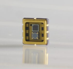
Marktech’s Next Gen Hermetic SMD ATLAS Packaged InGaAs Detectors
FOR IMMEDIATE RELEASE
Marktech Introduces New Line of 1.7µm & 2.6µm Extended InGaAs Detectors in Their Latest Hermetic Metal SMD (ATLAS) Packaging
March 20, 2023, Latham, NY, USA – Marktech Optoelectronics, a leading innovator in the photonics industry, is proud to announce the launch of its latest hermetic SMD packaged 1.7 and 2.6 micron InGaAs PIN photodiodes (PDs). These new detectors feature higher responsivity than most other InGaAs detectors on the market. The groundbreaking ATLAS brand package is designed to deliver exceptional performance and reliability for various applications, including spacecraft, aerospace, medical, defense, wearables, industrial factories, and more. In addition, this refinement of their ATLAS hermetic package has improved seal performance and reliability. A few orbiting satellites even contain space-qualified versions of the ATLAS package.
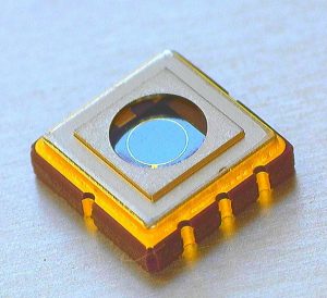
This new line of extended InGaAs PDs is specifically designed for harsh environments, providing unparalleled protection against water vapor, oxygen, and other gaseous contaminants that can negatively impact photodiode detector performance. In addition, the hermetic surface mount device (SMD) packaging ensures that these PDs maintain optimal functionality, even in the most demanding conditions.
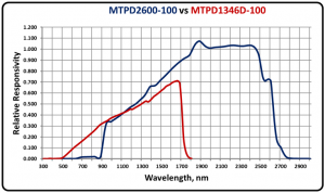
The 1.7µm and 2.6µm extended InGaAs detectors from Marktech offer enhanced sensitivity and excellent linearity, making them perfect for spectroscopy, gas sensing, moisture analysis, pyrometerers, and optical communication. In addition, the devices boast a high quantum efficiency and low dark current, ensuring optimal performance even in low-light conditions. 1.7µm cutoff InGaAs detectors can sense visible, near-infrared (NIR), and short-wave infrared (SWIR) light or wavelengths from 600nm to 1700nm. 2.6µm cutoff InGaAs detectors can sense NIR to extended SWIR light or wavelengths from 800nm to 2600nm. The ability to detect light in the SWIR wavelengths has opened up new applications in medical diagnostics, food sorting, and chemical analysis. SWIR wavelength also penetrates deeper into human tissue, which is helpful in medical diagnostics and wearables applications. The small footprint and shallow profile of Marktech’s ATLAS packaged InGaAs photodiode makes them compelling for wearable and point-of-care medical devices.
Marktech’s latest ATLAS Packaged InGaAs Photodiodes are available in 0.3mm, 1.0mm, and 1.5mm active areas. Larger active area photodiodes provide higher gain, while smaller active area detectors increase response speed. In addition, Marktech can manufacture custom active area size for projects with sufficient volume.

Benefits of ATLAS Packaged InGaAs Detector
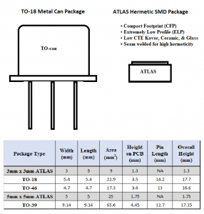
The ATLAS SMD package offers several advantages over traditional TO-can packaging, such as TO-39 and TO-18. While both are hermetic packages, the ATLAS is a surface mount device that allows pads to be soldered directly to a printed circuit board (PCB). TO-cans are through-hole mounted, which holes on the PCB to soldered connections. Surface mount technology is superior for high-volume production board assembly, offering several benefits compared to through-hole technology.
Key advantages of the ATLAS SMD packaged 1.7µm & 2.6µm InGaAs PIN photodiodes include:
- Compact Footprint (CFP) and Extremely Low Profile (ELP): These features make the ATLAS SMD package ideal for wearable and aerospace design projects, where photonics engineers are tasked with optoelectronics miniaturization and weight reduction, or improved size, weight, and power (SWaP).
- High Responsivity: With a greater responsivity than most other InGaAs PDs on the market, Marktech’s new detectors deliver improved performance for mission-critical applications.
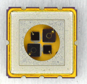
- Versatility & Integrity: Marktech’s InGaAs photodiodes are suitable for various applications, including spacecraft, aerospace, medical, defense, wearables, and industrial settings, where harsh conditions demand high-integrity component performance. Marktech’s detectors are single-element, quadrant, and multi-segment arrays. They can also be packaged with Marktech’s silicon photodiodes for broad detection from extended SWIR to UV wavelengths.
- Obscured Environment Sensing: When paired with the proper Marktech SWIR LED emitter, Marktech’s InGaAs detectors can sense through smoke, dust, water vapor (fog, steam, etc.), rain, and even select plastics. This ability to “see” or detect through dusty, concealed, or wet environments can be advantageous when developing advanced SWIR-based position, proximity, and other photoelectric sensors for mining, automotive, military, marine, paper & pulp, process plant, and security applications.
- Increased Assembly Productivity – The surface mount device (SMD) form factor improves assembly throughput compared to through-hole technology, which can lower the overall cost of a product in high-volume applications. In addition, the smaller footprint can ease the PCB board design process.
“With unexcelled performance and compactness, our ATLAS packaged 1.7 and 2.6 micron InGaAs PIN photodiodes represent a significant breakthrough in the photonics industry,” said Vince Forte, Chief Technology Officer of Marktech Optoelectronics. “Our focus on delivering high-quality, reliable components for mission-critical applications ensures that our customers can trust in the performance and durability of our products, even in the most challenging environments.”
Marktech’s commitment to innovation and quality has made it a trusted partner for customers across various industries. The new, expanding line of ATLAS packaged extended InGaAs detectors is another example of the company’s dedication to providing advanced solutions for today’s most demanding applications. In addition, Marktech manufactures a wide range of silicon photodiode detectors in their Simi Valley, CA factory. The combination of excellence in InGaAs and silicon photodiode technology allows Marktech to meet detection needs from UV to extended SWIR. Marktech can also design and fabricate custom InGaAs and silicon photodiodes, including custom complex, multi-segment arrays.
For more information on the ATLAS packaged 1.7µm & 2.6µm InGaAs PIN photodiodes, silicon photodiode, or other Marktech Optoelectronics detector products, please visit Marktech Detectors or email us at info@marktechopto.com. If you have an active project requiring advanced photodetection, submit an RFI or RFQ here – Contact Us.
About Marktech Optoelectronics: Marktech Optoelectronics is a leading provider of high-quality optoelectronic components, assemblies, and custom solutions for a diverse array of industries, including aerospace, medical, defense, and industrial. With a strong focus on innovation and customer satisfaction, Marktech is dedicated to delivering reliable, cutting-edge products designed to meet the unique needs of its customers. For more information, visit www.marktechopto.com.
Media Contact: Gary Kardys, Business Development Manager, g.kardys@marktechopto.com
See Us At Photonics West 2023
Happy New Year’s Wishes from the Marktech Optoelectronics team!
If you are attending SPIE Photonics West in January, then stop by our booth (#239) from January 30 thru February 3 at the Moscone Center in San Francisco, California. SPIE Photonics West is the world-renowned event for the photonics, optics, emitters, and detectors field.
Marktech Optoelectronics will be showcasing both their well-established and newly released products and capabilities, such as:
- Optical detectors (UV, Visible, & Infrared Detectors)
- Short Wave Infrared (SWIR) LEDs Emitters
- SWIR LEDs – 1020nm to 1720nm
- Extended SWIR LEDs – 1900nm to 2600nm – Coming in 2023
- Near Infrared (NIR) Emitters
- Visible LED Emitters – 400nm to 650nm
- Red dot LEDs, reticle LEDs, and alphanumeric LED micro-displays
- CREE-LED high-brightness LEDs in a wide range of forms:
- Through-hole, metal can, starboard, linear boards, and custom packages & assemblies
- SMD UV LEDs and Through-hole UV LEDs
- Advanced optoelectronic packaging capabilities
- Custom OEM Solutions – Optoelectronics Design, Engineering, Device Fabrication & Packaging
- Compound Semiconductor Materials
- Indium Phosphide (InP) Epitaxial Wafers for PIN Photodiodes
- APD Structured InP Epi-wafers
- Optoelectronic Chip Design & Fabrication (Photodiodes, Phototransistors, Custom Devices)
- Wide Spectral Range Optoelectronic Testing Services – Both Detectors & LED Emitters
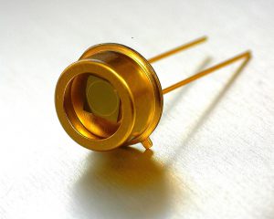
One of Several New 2.6µm InGaAs PIN Photodiode Innovations
Launching in 2023.
Marktech Optoelectronics, Inc. (www.marktechopto.com)(Marktech), is a privately-held and veteran-owned leading designer and manufacturer of standard and custom optoelectronics, including UV, visible, near-infrared (NIR), and short-wavelength infrared (SWIR) emitters, detectors, InP epi wafers, and other compound semiconductors.
Please drop by our booth or contact us any time if you:
- Have any technical or application questions or need assistance regarding any of your optoelectronic design projects
- Require validation of the optical characteristics (wavelength, power output, sensitivity) of your current optoelectronics components (emitters or detectors)
- Are you interested in learning more about Marktech’s cutting-edge InGaAs SWIR detectors, SWIR LED emitters, ATLAS hermetic SMD packaging, silicon photodetectors, chip-scale packaging (CSP), or multi-wavelength & multi-chip (MWMC) packaging
- Want to schedule a time to consult with our engineering experts at the Photonic West
If you have an urgent project or component questions: Contact Us.
Marktech Optoelectronics Introduces New 2.6µm Extended InGaAs Photodiode Photodetectors
Marktech’s New Extended 2.6µm Cutoff InGaAs Photodiode Photodetectors.
December 19, 2022 – Latham, NY, USA – Marktech Optoelectronics, Inc. (www.marktechopto.com)(Marktech), a privately-held leading designer and manufacturer of standard and custom optoelectronics, including UV, visible, near-infrared (NIR), and short-wavelength infrared (SWIR) emitters, detectors, InP epi wafers, and other compound semiconductors, today announced the release of two new indium gallium arsenide (InGaAs) photodiode photodetectors with extended 2.6µm wavelength responsivity cutoffs.
The new High Speed 2.6 micron InGaAs PIN photodiodes have sensitivity wavelength ranges of 600nm to 2600nm with active area diameters of 1.0mm. Marktech’s MTPD2601T-100 InGaAs photodiode is packaged in a TO-18 hermetic metal can with a flat lens. Our MTPD2601N-100 InGaAs component uses a TO-18 package with a domed lens. TO metal can packaging provides the highest protection against the ingress of vapor and moisture, which results in exceptionally reliable, high-lifetime InGaAs photodiode detectors.

Marktech’s InGaAs photodiode manufacturing partner in Japan, Optrans Corporation, is recognized as producing some of the industry’s highest integrity visible through SWIR detectors. These new products and many additional standard InGaAs photodiodes can be delivered in a few days from our distributors’ inventories, Digikey Electronics and Mouser Electronics.
In addition to standard InGaAs detectors, we can provide many additional services often required to rapidly move a project from the design to the finished product stage, such as:
- Detector and emitter selection
- Application and specification development
- InGaAs photodiode customization
- Package type selection and custom packages
- Electro-optical testing and troubleshooting
- Circuit and assembly design and build
InGaAs Photodiodes (InGaAs PDs)

Marktech’s lineup of advanced InGaAs photodiode detectors consists of several detector families or series based on their spectral sensitivity ranges:
- Vis-NIR-SWIR – 600nm to 1700nm spectral sensitivity
- NIR-SWIR-Extended SWIR – 800nm to 2600nm spectral sensitivity
While 1.7 µm and 2.6 µm are our standard offerings, Optrans can tailor the peak responsivity to wavelengths lower than 2.6µm for applications with sufficiently high annual volumes. InGaAs PIN photodiodes are available in various package types such as hermetically sealed metal cans (TO-5, TO-18, and TO-39), ceramic SAW packages, pigtail cans, 3mm molded plastic through-hole (flat lens or dome ceramic), and Marktech’s latest enhanced SMD packaging system, the hermetic ATLAS package. In addition, custom-engineered packaging to OEM specifications is available as well.
Extended InGaAs Advantages
Our InGaAs photodiodes provide high sensitivity, high speed, low noise, excellent linearity, high quantum efficiency, low-temperature coefficient of responsivity, low dark current, better shunt resistance, improved low operating temperature performance, and durability combined with an extended lifetime at a reasonable cost.

The high sensitivity of InGaAs detectors combined with low noise characteristics (high signal/noise ratio) in the NIR and SWIR wavelengths make InGaAs highly desirable for:
- Medical Devices and Wearables:
- Glucose monitoring (non-contact, optical)
- Blood alcohol monitoring
- Exhaled breath gas analysis
- Urinalysis
- Spectrometry:
- FTIR spectrometry
- Raman spectroscopy
- Tunable diode laser spectroscopy (TDLS)
- Scanning or dispersive NIR spectrometry
- Non-dispersive infrared (NDIR) spectroscopy
- Electroluminescence and fluorescence spectrometry
- Emerging infrared spectroscopy methods
- Temperature and flame detection
- Infrared pyrometry or non-contact radiation thermometers
- Flame and spark detection and regulation
- Moisture detection and compositional sorting
- Moisture meters (spectrophotometric)
- Precision agriculture
- Food sorting and food quality instruments,
- Plastics sorting and recycling
- Photonics test instrumentation:
- Coherent measurement systems
- IR laser diode characterization and monitoring
- Monitoring SWIR LEDs and illuminators
- Optical power meters
- Communication receivers in the O, L, and C bands
- Gas sensing
- Optical coherence tomography (OCT)
- LIDAR
In addition, InGaAs photodiodes have more thermal stability or a lower temperature coefficient of sensitivity (< 0.1% / K) over a broader range of wavelengths than silicon. As a result, our InGaAs photodiodes are ideal as the primary detector elements in non-dispersive spectrometers (Vis-NIR-SWIR), pyrometers, and medical diagnostic devices. Furthermore, Marktech’s infrared monitoring photodiodes can measure the optical power output of NIR and SWIR lasers and light sources, a critical element in the feedback and control of laser or illuminator output.
Custom Photodetectors to OEM Specs
We have extensive capabilities to design and manufacture custom photodetectors to OEM specifications from prototype to production volumes. Our capabilities in custom photodetector engineering and the manufacturing range include custom InGaAs photodiodes (wafers, die, packaged InGaAs PDs, and assemblies). In addition, Marktech can co-package InGaAs photodiodes with emitters, filters, thermoelectric coolers (TECs), and transimpedance amplifiers (TIAs). InGaAs photodiodes from Optrans Japan and silicon photodiodes from our Simi Valley plant are assembled in the same package to produce wide spectral band detectors – (SWIR/MIR to mid UVB). This technology makes hybrid InGaAs-silicon detectors with responsivities from 250nm to 2600nm feasible.
Consult with Us Today About Your Design Project
Marktech Optoelectronics and Optrans Corporation have vertically integrated capabilities to custom design and fabricate photodiode devices on wafers and then dice and package these photodiode chips with any required emitters, amplifiers, filters, and components for specific applications. This vertical integration allows Marktech to precisely control the performance and quality of the photodetectors and assemblies designed and manufactured for our customers.
Utilizing our advanced 2.6µm InGaAs photodetectors in new products under development will likely lead to breakthrough designs in many analytical instruments, medical diagnostics, and industrial sensing applications.
If you have specific technical or application questions regarding your photodetection design project or are just interested in learning more about Marktech’s InGaAs photodiodes, then please reach out to us through the following:
- Request for information (RFI) or request for quote (RFQ) form: Contact Us

Marktech Exhibiting Their Next Gen InGaAs Photodiode Detectors at the NYS Innovation Summit October 24th to 26th 2022
Marktech’s Next Gen InGaAs Photodiodes for
Visible through Short Wave Infrared Detection
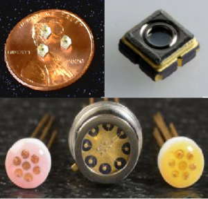
October 21, 2022 – Latham, NY, USA – Visit our booth at NYS Innovation Summit, the New York State’s world-renowned event for the innovations in advanced technologies and manufacturing. The event is held this year at the Buffalo Niagara Convention Center in Buffalo, NY.
Our InGaAs detectors have become a key enabling technology in many medical diagnostic, industrial position sensing, and chemical analysis applications.
Marktech Optoelectronics, a leader in the photonics, optics, emitters, and detectors field, will be showcasing both their well established and newly released products and capabilities such as:
- Photodetectors (optical detectors)
- Indium gallium arsenide (InGaAs) photodiode detectors with Vis to SWIR sensitivity
- Silicon Photodiode detectors with UV to NIR sensitivity
- Advanced optoelectronic packaging capabilities
- Chip-scale packaged (CSP) SWIR LEDs
- Multi-wavelength and multiple chip emitters and detectors
- ATLAS hermetic SMD packaging
- Infrared detectors and sources
- Near infrared (NIR) emitters and NIR detectors
- Short wave infrared (SWIR) emitters and SWIR detectors
- UV sources and detectors
- UV emitters (UVC LEDs, UVB LEDs, and UVA LEDs)
- UV enhanced silicon photodiode detectors
- Wide spectral range optoelectronic device testing services
- Custom OEM Solutions – Optoelectronics design engineering, device fabrication, and packaging to maximize your total cost benefit
- Indium Phosphide (InP) epitaxial wafers and compound semiconductor materials
- Optoelectronic chip design & fabrication (Photodiodes, Phototransistors, Custom Devices)
Marktech Optoelectronics, Inc. (www.marktechopto.com)(Marktech), is a privately-held and veteran-owned leading designer and manufacturer of standard and custom optoelectronics, including UV, visible, near-infrared (NIR), and short-wavelength infrared (SWIR) emitters, detectors, InP epi wafers, and other compound semiconductors.
Please drop by our booth or contact us any time if you:
- Have any technical or application questions or need assistance regarding any of your optoelectronic design projects
- Require validation of the optical characteristics (wavelength, power output, sensitivity) of your current optoelectronics components (emitters or detectors)
- Are interested in learning more about Marktech’s ATLAS hermetic SMD packaging, silicon photodetectors, InGaAs detectors, chip-scale packaged (CSP) SWIR LED emitters and multi-wavelength or multi-chip packaging
- Want to schedule a time to consult with our engineering experts at the Photonic West
If you have an urgent project or component questions, contact our application engineers at: info@marktechopto.com or call us at 1-518-956-2980.
Marktech Optoelectronics Announces New InGaAs Quad and Array Photodiodes for Laser Alignment and Position Sensing Applications
New InGaAs Quadrant and Array Photodiodes from Marktech Optoelectronics
September 21, 2022 – Latham, NY, USA – Marktech Optoelectronics, Inc. (www.marktechopto.com)(Marktech), a privately-held leading designer and manufacturer of standard and custom optoelectronics, including UV, visible, near-infrared (NIR), and short-wavelength infrared (SWIR) emitters, detectors, InP epi wafers, and other compound semiconductors, today announced their offering of cutting-edge InGaAs quadrant and array photodiodes for laser alignment and position sensing applications.
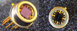
“Quads” or quadrant photodiodes (QPDs) are segmented photodiode position sensing detectors (PSD, AKA position sensing diodes) with four planar diffused photodiode elements, which are monolithic or on the same silicon or InGaAs chip. Marktech Optoelectronics quad photodiodes have low dark current, high resolution or precision, high accuracy, high response with low noise (high S/N ratio), wide spectral ranges, good frequency bandwidth, excellent dynamic range, minimal element spacing, low operating voltages, high shunt resistance, and large active areas.
Two-segment, dual element, or bi-cell photodiodes are another type of position sensing device commonly incorporated into alignment or positioning systems. While quadrant photodiodes can sense position along two dimensions or the X & Y axes, bi-element photodiodes align or position along one dimension or axis.
Marktech’s four-element photodiode arrays or quad detectors provide flawless performance in laser alignment and nanopositioning applications. Quadrant photodiodes (QPDs) or quadrant position sensitive detectors typically have resolutions as low as 10nm using beams with optical powers from 10 to 100microWatts (Ref 1). Quads can be used in auto-collimators for laser alignment, optical trackers, scanning probe microscopes, stage positioners, surface profilometers, mask aligners, beam centering systems, space sun sensors, ellipsometers, optical tweezers, tilt sensors, high accuracy displacement sensors, and other ultra-precision positioning applications. The fast response and wide operational bandwidth of QPDs have made these positioning devices dominant in the atomic force microscope (AFM) industry (Ref 2). Satellite communication systems can benefit from quadrant photodiodes as well. For example, quadrant photodiodes are critical components in quadrant photoreceiver (QPR) front-end devices for inter-satellite laser interferometry.
InGaAs Photodiode Arrays
Both bi-cell and quadrant photodiodes are photodiode arrays (PDAs) with two (1X2) and four (2X2) elements, respectively. Bi and quad PDs are suitable for alignment or position sensing over a small beam displacement or position range. For laser or light beam position sensing over a more extensive range, longer, multi-element photodiode arrays are necessary. Marktech Optoelectronics can manufacture custom multi-element linear (one dimensional, 1D) and area (two dimensional, 2D) photodiode arrays with many segments for dispersive spectroscopy, refractometry, distance or range finding (triangulation position sensing), interferometry, and particle analyzers. Many photodiode array applications require custom-designed arrays and OEM custom integration, one of Marktech’s industry-leading capabilities. Marktech’s detector experts have designed and manufactured photodiode arrays with 2, 4, 16, 20, 32, 64, and more elements.

Advantages of InGaAs Position Sensitive Detectors
InGaAs quadrant, bi-segment, and multiple segment array position-sensitive detectors have several advantages over imaging sensors (CCD, CMOS, focal plane arrays, etc.), such as high position resolution, fast response time, lower cost, and straightforward signal conditioning circuit designs. In addition, InGaAs linear arrays are employed in pulsed laser or direct time of flight (TOF), phase shift or indirect time of flight (TOF), and triangulation position sensors.
InGaAs positioning sensitive detectors have a further advantage over silicon PSDs in their ability to sense eye-safe laser wavelengths in the NIR and SWIR bands. In addition, specific SWIR wavelengths can “see” or detect through plastics, fog, smoke, or moisture, which is an advantage over visible and NIR PSDs. For example, water is opaque when viewed at specific wavelengths such as 1400nm, so an InGaAs PSD with a 1400nm SWIR LED emitter could sense water levels in a plastic container or tank. In a factory application, InGaAs detectors with 800nm to 2600nm sensitivity should have no or fewer false triggering events from high brightness LED work lights and other stray light sources in the visible band. Detectors with ambient light immunity are beneficial in triangulation position sensing systems and LiDAR devices.
InGaAs Wavelength Sensitivity Range
Our InGaAs quadrant photodiodes and photodiode arrays have a wavelength sensitivity range from 600nm to 2600nm (600nm to 1700nm for our 1.7µm InGaAs PDs and 800nnm to 2600nm for our 2.6 µm InGaAs PDs). Our silicon quadrant photodiodes and photodiode arrays have a wavelength sensitivity range from 250nm to 1100nm. These die can be packaged individually in a variety of hermetically sealed TO packages or integrated into a custom package (PLCC, COB, hermetic SMD, ceramic carrier, etc.) to suit your specific application and pin-out design specs. Marktech has several class 100 cleanrooms for the advanced packaging and assembly of custom InGaAs and silicon photodiode devices on rigid PCBs, flexible circuits, and OEM-specific designs.

Custom silicon quadrant photodiode array
made in Marktech’s factory in Simi Valley, CA.
Custom InGaAs Photodiodes and Packaging
Marktech routinely manufactures custom photodetectors to OEM specifications from prototype to production volumes. The range of Marktech’s custom photodetector engineering and manufacturing, including custom InGaAs photodiodes:
- Wafer-level device design
- Semiconductor wafer fabrication of InGaAs photodiode devices
- Conversion of InGaAs devices on wafers to die or chips
- Packaging of InGaAs die in:
- Standard packages (TO can, PLCC, ceramic, etc.)
- Proprietary packages (ATLAS hermetic SMD)
- OEM-specific custom packages
Marktech can co-package InGaAs photodiodes with emitters, filters, and transimpedance amplifiers (TIAs). Marktech’s U.S. factory in Simi Valley, CA, has a similar level of competency in producing silicon photodiode detectors. In addition, silicon and InGaAs photodiodes are assembled in the same package for wide spectral band detection applications (MT03-041 TO-39 Metal Can Flat Lens and MT03-047 Ceramic SAW Package).
Marktech Optoelectronics has vertically integrated capabilities to custom design and fabricate InGaAs photodetector and photodiode array devices on wafers and then dice and package these photodiode chips with any required emitters, amplifiers, filters, and components for specific applications. This vertical integration allows Marktech to precisely control the performance and quality of the photodetectors and assemblies designed and manufactured for our customers.
Consult with Us Today About Your Design Project
Using Marktech Optoelectronics advanced InGaAs photodetectors in new products under development will likely lead to breakthrough designs in many analytical instruments, medical diagnostics, and industrial sensing applications.
If you have specific technical or application questions regarding your optoelectronics design project or are just interested in learning more about Marktech’s InGaAs and silicon photodiodes, then please reach out to us through the following:
- Contact our application engineers: info@marktechopto.com
- Request for information (RFI) or request for quote (RFQ) form: Contact Us
- For major photodiode engineering projects, contact our U.S. factory directly:
Vince Forte, Chief Technology Officer, v.forte@marktechopto.com
Barry Jones, Business Unit Manager b.jones@marktechopto.com

Marktech Optoelectronics Announces Latest Lineup of Advanced Silicon Photodiode Photodetectors
Marktech’s Latest Lineup of Advanced Silicon Photodiodes
March 22, 2022 – Latham, NY, USA – Marktech Optoelectronics, Inc. (www.marktechopto.com)(Marktech), a privately-held and veteran-owned leading designer and manufacturer of standard and custom optoelectronics, including UV, visible, near-infrared (NIR), and short-wavelength infrared (SWIR) emitters, detectors, InP epi wafers, and other compound semiconductors, today announced their latest lineup of advanced silicon photodiode photodetectors.
Marktech’s silicon photodiode manufacturing facility Simi Valley, California has one the shortest delivery lead times in the photodetector industry for standard and custom photodiodes. Marktech can cross many competitor’s silicon photodiodes with a MADE IN THE USA product having specifications matching or exceeding the competitive specifications. After prototype approvals, custom photodiodes are typically delivered in a highly competitive time frame versus the typical 6 to 8 months from other leading photodiode manufacturers. In addition, many standard silicon photodiodes can be delivered from our standard inventory in a few days through our distributor websites, Digikey Electronics and Mouser Electronics.
Silicon Photodiode (SiPDs)
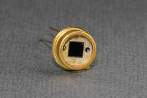
Marktech’s lineup of advanced silicon photodiode detectors consist of several detector families or series based on their spectral sensitivity ranges:
- General Purpose (Series 8) – 350 to 1100nm spectral sensitivity
- UV Enhanced (Series 4) – 300 to 1100nm spectral sensitivity
- IR Enhanced Peak (Series 14) – 350 to 1100nm spectral sensitivity
- UV & IR Enhanced (Series 11) – 250 to 1100nm spectral sensitivity
Silicon PIN photodiodes are available in various package types such as hermetically sealed metal cans (TO-5, TO-18, and TO-39), ceramic SAW packages, pigtail metal cans, and 3mm molded plastic through-hole (flat lens or dome ceramic). Custom packaging to OEM specifications is available as well.
Marktech’s Si photodiodes provide high sensitivity, low noise, excellent linearity, high quantum efficiency, and durability combined with an extended lifetime at a reasonable cost. Our UV Enhanced silicon photodiodes are ideal for monitoring the consistency of UV light sources for curing inks, resins, adhesives, sealants, and 3D printing stereolithography materials. In addition, Marktech’s IR emitters combined with our IR detectors (IR Peak silicon photodiodes) are the perfect solution in many industrial sensing applications such as proximity, linear position, time-of-flight (TOF) distance or range, and angular or rotary position sensors. Additional applications include optical power meters, color sensors, optical receivers, daylight detectors, oximeters, pulse monitors, particle analyzers, and smoke detectors.
Avalanche Photodiodes (APDs)
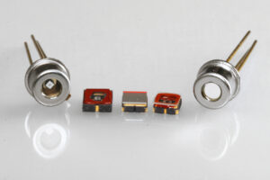
Marktech’s avalanche photodiodes (APDs) are perfect for high speed, short pulse,
and low light level detection between 400 to 1100nm. They have optimal peak responses in the NIR band at 800nm or 905nm. Marktech APDs have low dark current, high internal gain at low bias voltage, and significantly higher sensitivities, especially in the near-infrared (NIR) spectral range, compared to standard photodiodes. They also have fast rise times as low as 300 ps, frequency response to 1 GHz, and a low breakdown voltage of 120V-200V. All Marktech APD products are also RoHS compliant.
Multiple Si APD customization options include operational voltage selection, wavelength-specific band-pass filtering, hybridization, and custom packaging. Custom package options include hermetically sealed TO metal cans, cost-effective SMD (LCC) types, proprietary seam welded ATLAS SMD, and other package types developed to OEM specifications.
Marktech silicon APDs can provide performance nearly equivalent to photomultipliers but in a more durable, reliable, and lower-cost semiconductor product. As a result, Marktech APDs can detect weaker light intensities accurately in applications where higher bandwidth or internal gain may be required. Competitive photodetectors option fall short due to higher preamplifier noise levels.
Marktech offers the industry’s largest selection of standard off-the-shelf Silicon APDs for immediate customer delivery. In addition, our California factory routinely manufactures prototypes to OEM production volumes of standard and custom silicon APDs. Marktech’s standard silicon APDs are available through our global distribution partners, DigiKey Corporation and Mouser Electronics.
Silicon Phototransistors
Marktech offers a broad line of silicon phototransistors in various package types ranging from small metal can to ceramic packages. Marktech’s silicon phototransistors have a spectral sensitivity in the 400 nm to 1100 nm range or special UV enhanced silicon chips with sensitivity in the lower UV-A range. They are useful in applications requiring very high sensitivity, uniform response, and increased reliability, such as card readers and optical sensors. In addition, our Simi Valley Si photodiode plant can manufacture custom active areas and multi-element chips to suit your application.
Silicon Photodiode Arrays (Si PDAs)
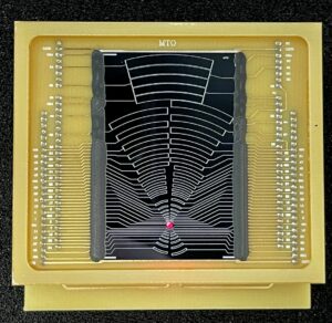
Silicon photodiode arrays have multiple photodiode elements fabricated on the same substrate and package. The photodiode arrays range from bi detectors (two segments), quad detectors (four elements), multiple element linear arrays, and complex multi-element area arrays.
Photodiode arrays are critical components in sensors and instruments for position sensing, laser alignment, spectroscopy, and particle analysis. For example, Marktech’s four-element photodiode arrays or quad detectors are perfect laser alignment applications. In addition, our linear photodiode arrays are ideal for position detection, spectrometry, refractometry, and other sensor or instrument applications.
InGaAs Photodiodes (InGaAs PDs)
In addition to our high-performance silicon photodiodes, Marktech manufactures InP PIN photodiodes using InGaAs/InP technology. These InGaAs PIN photodiodes have a spectral sensitivity in the 600nm to 2600nm range for applications requiring low dark current, high speed, and sensitivity, such as fiber optics and optical communications, detection of SWIR emitters. In addition, Marktech’s InGaAs PIN photodiodes do not require integrated thermal electric (TE) coolers, which reduces costs and improves overall efficiency.
Multispectral Broadband Photodiodes (MB PDs)
Marktech Optoelectronics broadband photodiode provides multispectral sensitivity capable of detecting from UV to SWIR wavelengths (250nm to 2600nm). Marktech’s broadband photodiodes combine a UV detection enhanced silicon photodiode and an InGaAs photodiode. The broadband photodetector is available in a TO-39 metal can package (MT03-041) and a ceramic SAW package (MT03-047). Marktech UV to SWIR photodetectors find applications in the medical diagnostic, industrial sensing, optical communications, and security industries.
Custom Photodetectors to OEM Specs
Marktech has extensive capabilities to design and manufacture custom photodetectors to OEM specifications from prototype to production volumes. The range of Marktech’s custom photodetector engineering and manufacturing include:
- Custom silicon photodiodes (Wafers, die, and packaged SiPDs)
- Custom photovoltaic silicon PIN photodiodes
- Custom silicon photoconductive PIN photodiodes
- Custom silicon avalanche photodiodes
- Custom InGaAs photodiodes
- Custom silicon and InGaAs photodiode arrays
- Custom photodetector packaging
- Photodetector co-packaged with additional components:
- Photodiodes combined with filters
- Photodiodes combined with transimpedance amplifiers (TIAs)
- Photodiodes combined with thermal electric coolers (TECs)
- Photodiodes combined with LED emitters
- Multiple photodiodes with varying spectral ranges
- Custom photodetector assemblies (boards, flexible circuits, etc.)
Marktech’s newest manufacturing facility in Simi Valley, CA produces our advanced SiPDs. The California plant has a class 100 cleanroom and advanced packaging and assembly lines.
 Marktech has a state-of-the-art optoelectronics laboratory for inspection and quality assurance testing of both detectors and emitters. Marktech routinely employs this capability to assist customers in troubleshooting problems with competitive SiPDs and developing OEM requirement specifications.
In addition, Marktech Optoelectronics can assemble endless combinations of multiple UV, visible, NIR, and SWIR emitters or LEDs photodiode detectors with the same package. Unique combinations of LED light sources and photodiode detectors are instrumental in developing sensors and instruments for detecting and quantifying specific chemicals, dissolved gases, and other biomarkers in process plant, clinical chemistry, wearable medical device, blood gas analysis, and point of care diagnostics.
Consult with Us Today About Your Design Project
Marktech Optoelectronics has vertically integrated capabilities to custom design and fabricate silicon photodetector and silicon photodiode array devices on wafers and then dice and package these photodiode chips with any required emitters, amplifiers, filters, and components for specific applications. This vertical integration allows Marktech to precisely control the performance and quality of the photodetectors and assemblies designed and manufactured for our customers.
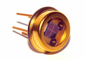
Using Marktech Optoelectronics advanced silicon photodetectors in new products under development will likely lead to breakthrough designs in many analytical instrument, medical diagnostics, and industrial sensing applications.
If you have specific technical or application questions regarding your optoelectronics design project or are just interested in learning more about Marktech’s silicon photodiodes, then please reach out to us through the following:
- Contact our application engineers: info@marktechopto.com
- Request for information (RFI) or request for quote (RFQ) form: Contact Us
- For major photodiode engineering projects, contact our U.S. factory directly:
Barry Jones, Business Unit Manager b.jones@marktechopto.com
Mouser Electronics and Marktech Optoelectronics Announce Global Distribution Agreement
Mouser Electronics, Inc., the authorized global distributor with the newest semiconductors and electronic components, announces a global distribution agreement with Marktech Optoelectronics, a leading designer and manufacturer of standard and custom optoelectronics components as well as assemblies. According to the agreement, which commenced in 2021, Mouser will offer customers Marktech Optoelectronics’ range of emitters and photodiodes for applications including night vision, safety equipment, fiber optics, industrial automation, chemical analysis, and currency validation.
In the infrared wavelength ranges, Marktech is a vertically integrated manufacturer growing epitaxy InP wafers, fabricating InGaAs detector and emitter chips, packaging chips, and even producing completed assemblies for some OEM customers. Marktech has leading-edge packaging capabilities with the ability to package die in molded plastic through-hole, SMD, chip-scale, TO can, chip on board (COB), and their proprietary seam-welded hermetic ATLAS package. Marktech’s advanced packaging capabilities can produce multiple die components including designs with multi-wavelength emitters, multiple detectors for broadband detection, and emitter-detector combinations.
Marktech also designs and produces silicon photodiode detectors, avalanche photodiodes (APDs), phototransistors, and photodiode arrays (PDAs) for applications including colorimeters, currency validation, industrial sensing (proximity, edge detection, light barriers, encoders), bar code readers, fast receivers, photometers, optical test equipment, smoke detectors, optical switches, refractometers, fluorometers, and NIR spectrometers. Marktech’s silicon photodiode photodetectors are MADE in the USA in their Simi Valley, CA manufacturing plant.
Marktech’s shortwave infrared (SWIR) emitters and detectors are an ideal solution for material and chemical spectroscopy, offering high-speed light emission in ranges not easily perceived by standard detectors. The SWIR emitters are designed for high-power applications and feature operating currents ranging from 20mA to 350mA. Boasting a wide beam angle and high reliability, the SWIR emitters include both through-hole and surface mount packages with wavelengths from 1020nm to 1720nm.
The near infrared (NIR) emitters and detectors offer exceptional optical/mechanical axis alignment, making them a suitable choice for high-precision applications including bar code readers, fiber optics, proximity sensors, optical switches, and position sensors. The near-infrared emitters feature a peak emission wavelength range of 720nm to 950nm, and they are frequently used in the agriculture, banking, medical, security, automation, and communications industries.
Marktech’s high-power SMD UV emitters combine low thermal resistant material with state-of-the-art SMD design to deliver super high power output. The emitters are ideal for UV curing, disinfection, and chemical and biological analysis, as well as printing, coating, and counterfeit detection. The high-power SMD UV emitters offer a peak emission wavelength range of 235nm to 400nm. UV detectors are also available with spectral ranges from 200nm to 400nm.
To learn more, visit https://www.mouser.com/manufacturer/marktech-optoelectronics/.
As a global authorized distributor, Mouser offers the world’s widest selection of the newest semiconductors and electronic components — in stock and ready to ship. Mouser’s customers can expect 100% certified, genuine products that are fully traceable from each of its manufacturer partners. To help speed customers’ designs, Mouser’s website hosts an extensive library of technical resources, including a Technical Resource Center, along with product data sheets, supplier-specific reference designs, application notes, technical design information, engineering tools, and other helpful information.
About Mouser
In 2021, Mouser Electronics, a Berkshire Hathaway company, is an authorized semiconductor and electronic component distributor focused on New Product Introductions from its leading manufacturer partners. Serving the global electronic design engineer and buyer community, the global distributor’s website, mouser.com, is available in multiple languages and currencies and features more than 5 million products from over 1,100 manufacturer brands. Mouser offers 27 support locations worldwide to provide best-in-class customer service in the local language, currency, and time zone. The distributor ships to over 630,000 customers in 223 countries/territories from its 1 million-square-foot, state-of-the-art distribution facilities in the Dallas, Texas, metro area. For more information, visit https://www.mouser.com.
About Marktech Optoelectronics
Marktech Optoelectronics is a privately held, VOSB-certified, leading designer and manufacturer of optoelectronic components and assemblies, including UV, visible, near-infrared, and short-wave infrared (SWIR) emitters, detectors, InP epiwafers, and other materials.
Trademarks
Mouser and Mouser Electronics are registered trademarks of Mouser Electronics, Inc. All other products, logos, and company names mentioned herein may be trademarks of their respective owners.
Marktech Expands Their Innovative Optoelectronics Packaging with Chip-scale SWIR LEDs, Multichips & ATLAS Hermetic SMD
LATHAM, NY, US, October 27, 2021 / — Marktech Optoelectronics, Inc. (www.marktechopto.com)(Marktech), a privately-held and veteran-owned leading designer and manufacturer of standard and custom optoelectronics, including UV, visible, near-infrared (NIR), and short-wavelength infrared (SWIR) emitters, detectors, InP epi wafers, and other compound semiconductors, is expanding their innovative optoelectronic packaging with:
- Chip-scale SWIR LEDs
- Multi-wavelength and Multiple Chip Emitters and Detectors
- ATLAS Hermetic SMD Packaging
Chip Scale Packaged SWIR LED Emitters – An Industry First
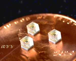
The availability of SWIR LEDs or emitters in a chip-scale packaged form factor is an industry first. The compactness of the new CSP SWIR LEDs is impressive. A dozen or more of Marktech’s CSP SWIR emitters would fit on the surface of a penny.
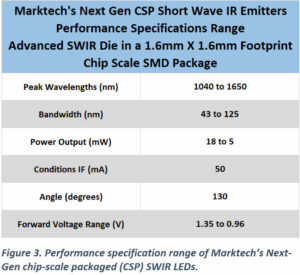
These Next-Generation CSP short wave IR emitters have an extremely small footprint compared to conventional short wave IR emitters in surface mount device (SMD) or transistor outline (TO) metal can packages. The new short wave IR emitters consist of a high-performance SWIR chip in an extremely compact 1.6mm x 1.6mm x 1.6 mm cube-shaped SMD package with two lead pads. The flat lens design produces a wide or Lambertian radiation pattern with beam angles of 130°. The high-performance CSP short wave infrared emitter products are available in wavelengths ranging from 1040 to 1650 nm.
1020nm and 1720nm CSP short wave IR emitters are available using conventional, lower power output SWIR chips. Marktech Optoelectronics can provide additional engineering and testing to deliver specific wavelengths and forward voltages as well as tighter power output bands through sorting or epi material customization. In machine vision and inspection, SWIR bandpass filters or longpass filters can be used in conjunction with SWIR light sources and SWIR cameras to adjust the bandwidth or pass only the SWIR light required for imaging – thereby increasing SWIR image contrast and resolution.
The major performance attributes of Marktech’s Chip Scale Packaged SWIR LED Emitters include:
- Up to double the power output – up to 2X the power output compared to older SWIR LED chips
- Compact CSP LED size enables high stacking density on a printed circuit board (PCB)
- Improved SWIR component reliability
- Increased SWIR component lifetime or mean time between failures (MTBF)
- Lower thermal resistance compared to plastic leaded chip frame (PLCC) SMD SWIR LEDs
Marktech Multi-wavelength and Multiple Chip Emitters and Detectors
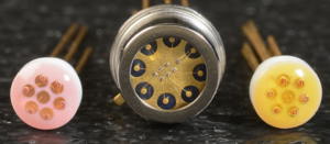
In addition to advanced SWIR LED emitters, Marktech has multichip packaging capabilities, which can combine various NIR and SWIR LEDs and detectors within the same package for multispectral applications such as LED LIDAR and optical ranging sensors. Marktech also provides complementary products such as short wave IR InGaAs detectors for applications requiring both a SWIR light source combined with a SWIR sensor. A series of UV to SWIR emitters in a multichip package can provide a light source with a wide range of wavelengths for spectrometry and hyperspectral imaging. Marktech can bond from 2 to 144 die within the same package.
In summary, Marktech’s multichip packaging processes can provide within the same compact, surface mount, or hermetic package:
- Multiple wavelength emitters or LEDs with wavelengths from 255 nm to 1720 nm
- Multiple spectral range detectors
- Combinations of multiple emitters and detectors
Marktech Optoelectronics can also provide chip-on-board (COB) packaging where multiple chips populate a ceramic or aluminum cored metal clad printed circuit board (Al-cored MCPCB). Chip-on-board (COB) might be the best choice to maximize heat dissipation when a design requires a very dense packaging of multiple emitters or LEDs. Aluminum core COB boards are available in linear, ring, and starboard formats.
ATLAS Hermetic SMD Packaging
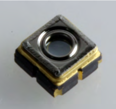
Marktech’s CSP SWIR LED joins a growing family of advanced emitters and detectors in enhanced packaging such as Marktech’s ATLAS packaged line of LEDs, photodetectors, and emitter-detectors. The Marktech revolutionary ATLAS package combines the hermetic characteristics of a TO metal can packaged optoelectronic device with the great manufacturability associated with surface mount devices (SMDs). ATLAS packaged optoelectronic components are available in 3mm x 3mm and 5 mm x 5mm size. The ATLAS hermetic SMD packaging is constructed using a glass to ceramic seam welded process to provide water vapor and oxygen ingress protection.
Multiple wavelength LEDs or emitters and photodetectors can be packaged in the larger ATLAS package. ATLAS is an ideal package for applications requiring extreme sensitivity and high reliability because the seam-welded metal-to-ceramic seal in the ATLAS package prevents the ingress of water vapor and oxygen into the cavity holding the LED chips and photodetectors.
Using the ATLAS package technology, Marktech can engineer hermetic surface mount device (SMD) packages to hold and protect a wide range of SWIR LEDs, SWIR sensors, and custom LED-sensor combinations to your specific SWIR design application requirements in wavelengths ranging from 310 nm to 2600 nm. The hermetically sealed weld on the ATLAS ceramic SMD package provides excellent protection of chips from damaging high humidity environmental conditions. Marktech also has begun to offer standard or catalog products in the hermetic ATLAS package, such as Marktech’s MTSM1346SMF1-100 High-Speed InGaAs PIN Photodiode, which delivers IR to SWIR (600 nm to 1750 nm) photodetection.
Marktech’s Advanced Optoelectronic Packaging Family
In summary, Marktech’s advanced optoelectronic packaging family includes:
- Chip scale packaging – CSP LED or CSP emitters
- Hermetic TO-can packaging
- ATLAS Hermetic SMD Packaging – ingress proof optoelectronics
- Chip-on-board (COB) packaging using ceramic or Al-cored metal-clad PCB (MCPCB)
- Multiple chip packaging – Multiple wavelength emitters, photodetectors, and emitter-photodetector combinations
The high compactness and high power output of Marktech’s new CSP infrared LEDs, multichip packages, and ATLAS hermetic SMDs will enable engineers to shrink and enhance their optoelectronic design projects. Their adoption in product development projects will lead to breakthrough designs in many industrial applications.
If you have specific technical or application questions regarding your optoelectronic design project or are just interested in learning more about Marktech’s advanced packaging, emitters, and detectors, then please contact our application engineers: info@marktechopto.com
Gary Kardys
Marktech Optoelectronics
+1 518-956-2980
g.kardys@marktechopto.com
Short Wave Infrared Emitters in a Chip Scale Package (CSP) Introduced by Marktech Optoelectronics – An Industry First
September 1, 2021 – Latham, NY, USA – Marktech Optoelectronics, Inc. (www.marktechopto.com)(Marktech), a privately-held and veteran-owned leading designer and manufacturer of standard and custom optoelectronics, including UV, visible, near-infrared (NIR), and short-wavelength infrared (SWIR) emitters, detectors, InP epi wafers, and other compound semiconductors, today announced the introduction of chip-scale packaged (CSP) short wave infrared emitters (also known as CSP SWIR LEDs, CSP short wave IREDs, or CSP SWIR emitters).
The availability of SWIR LEDs or emitters in a chip-scale packaged form factor is an industry first. The compactness of the new CSP SWIR LEDs is impressive. In fact, a dozen or more of Marktech’s CSP SWIR emitters would fit on the surface of a penny.
CSP SWIR LED Performance Features
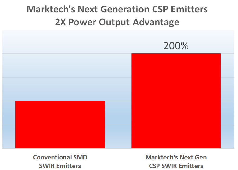 These Next-Generation CSP short wave IR emitters have an extremely small footprint compared to conventional short wave IR emitters in surface mount device (SMD) or transistor outline (TO) metal can packages. The new short wave IR emitters consist of a high-performance SWIR chip in an extremely compact 1.6mm x 1.6mm x 1.6 mm cube-shaped SMD package with two lead pads. The flat lens design produces a wide or Lambertian radiation pattern with beam angles of 130°. Marktech’s chip-scale packaged SWIR LEDs are both RoHS and REACH compliant. The high-performance CSP short wave infrared emitter products are available in wavelengths ranging from 1040 to 1650 nm. The specific SWIR LED wavelengths available include:
1020nm and 1720nm CSP short wave IR emitters are available using conventional, lower power output SWIR chips. Marktech Optoelectronics can provide additional engineering and testing to deliver specific wavelengths and forward voltages as well as tighter power output bands through sorting or epi material customization. In machine vision and inspection, SWIR bandpass filters or longpass filters can be used in conjunction with SWIR light sources and SWIR cameras to adjust the bandwidth or pass only the SWIR light required for imaging – thereby increasing SWIR image contrast and resolution.
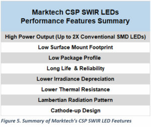
The major performance attributes of Marktech’s CSP short wave infrared emitters include:
- Up to double the power output – High-performance SWIR LED dies in the CSP package provide up to 2X the power output compared to older, conventional SWIR LED chips
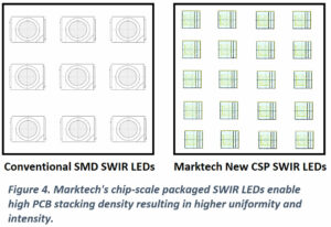
- Compact CSP LED size enables high stacking density on a printed circuit board (PCB) due to the small 1.6mm X 1.6mm footprint
- Improved SWIR component reliability
- Increased SWIR component lifetime or mean time between failures (MTBF)
- Lower thermal resistance compared to plastic leaded chip frame (PLCC) SMD SWIR LEDs
 Reliability increases originate from several facets of the chip-scale packaged SWIR LED design. First, the advanced SWIR die itself contributes to improved reliability.
Second, Marktech’s CSP packaged SWIR LED SMD combines aspects of high power emitter packaging with typical LED chip-scale packaging to create a new high power chip-scale package SMD (HP CSP SMD).
The high-power (HP) SWIR LED packages utilize a low thermal resistance ceramic submount to rapidly dissipate heat. The high thermal resistance in plastic leaded chip carriers (PLCC) SMD LEDs results in poor heat dissipation and reduced performance.
Ceramics are typically 10 times higher in thermal conductivity compared to plastics. The ceramic submount in the Marktech’s CPS SWIR LED provides a powerful “heat slug” for reduced thermal resistance, enhanced heat dissipation, and an overall improvement in reliability. The large contact area of the anode and cathode pads on the bottom of the CSP SWIR SMD package provide lower resistance electrical and thermal conduction paths.
CSP SWIR LED Applications
Short wave infrared emitters have become important components empowering advanced designs in aerospace, automotive, medical, imaging, spectroscopy, microscopy, night vision, security, defense, agriculture, semiconductor, industrial, and communications applications.
Certain materials such as silicon, which are normally opaque in the visible band, are transparent in the SWIR wavelength region. Some materials, biological samples, and organic compounds have enhanced contrast or exhibit fluorescence when imaged in the SWIR band. In medical applications, SWIR imaging systems have been developed to detect cancers, non-invasively measure blood glucose, and diagnose inner ear conditions (otoscopes).
In semiconductor applications, SWIR microscopes and inspection systems more efficiently detect defects on the surface of silicon wafer surfaces. SWIR vision systems and digital sorters utilize the contrast differences between various materials and natural compounds to detect contamination in grains, nuts, seeds, and other food products.
Shadowing is more pronounced under SWIR light and therefore the shape and form of parts and their features are more easily determined, which is useful for machine vision, surface metrology, and optical gaging system applications.
SWIR cameras, SWIR microscopes, SWIR spectrometers, SWIR endoscopes, SWIR hyperspectral machine vision systems require consistent, spatially homogeneousness SWIR light sources with high power output or intensity. The combination of high power output in a denser concentration on a PCB or ring board has the potential to improve image quality, signal-to-noise ratio, and detection efficiency in spectroscopy or chemical analysis, microscopy, imaging, wafer inspection, and vision systems. High uniformity SWIR light source illumination of a surface can be attained at short working distances with denser PCB stacking of Marktech’s compact CSP SWIR LEDs.
SWIR cameras, SWIR detectors, and SWIR LIDAR systems can “see” through obscured environments such as rain, fog, clouds, plastics, and organic materials. Marktech’s SWIR InGasAs detectors in combination with CSP SWIR LEDs can provide compelling advantages in collision avoidance and autonomous vehicle detection applications in the automotive, aerospace, defense, and security industries. Unlike conventional thermal imagers and infrared cameras for night vision, SWIR camera image sensors and SWIR detectors are not overwhelmed or “blinded” by daylight infrared radiation from the sun, which means SWIR cameras and SWIR detectors can be used day and night in surveillance, agricultural crop sensing, and defense applications.
CSP SWIR LED Design Advantages
These new SWIR components are ideal for optoelectronic design projects demanding increased miniaturization or compactness combined with enhanced longevity, dependability, and power output performance.
The potential design benefits of Marktech’s CSP short wave IR emitter technology includes:
- Miniaturization – the small footprint and reduced height of CSP SWIR LEDs will allow design engineers to reduce the size of SWIR cameras, SWIR spectrometers, SWIR microscopes, SWIR machine vision systems
- Higher Intensity – the ability to use more SWIR LEDs per unit area in combination with the higher power output of each advanced SWIR emitter results in an increase in total power output and intensity.
- Improved Uniformity – the use of a larger number of SWIR LEDs across an area should provide a more uniform short wave infrared light source even at closer working distances.
- Increased System Reliability – the higher lifetime and reliability of Marktech’s CSP SWIR emitters should contribute to improved system reliability.
 For multispectral camera and machine vision applications, combinations of NIR-vis and SWIR broadband LEDs can be packaged to provide light sources custom matched to the spectral response of specific hyperspectral cameras. CSP multispectral LED light sources have the additional advantage of lower operating temperature and power consumption compared to hyperspectral Halogen light sources.
CSP SWIR LED Thermal Management and Board Design
While CSP SWIR LEDs have many performance advantages, chip-scale packaged LED SWIR designs with high packing densities can overcome the heat dissipation ability of FR4 printed circuit board materials. When compared to visible light emitters, SWIR LEDs tend to be less efficient and will generate more heat under the same current or power loads. Printed circuit boards with high stacking densities of SWIR LEDs should have an array of thermal vias or even a thermal pad and additional heat sinks on the underside to help improve the thermal performance. A ceramic or aluminum cored metal clad printed circuit board (Al-cored MCPCB) or a chip-on-board (COB) might be the best choice to maximize heat dissipation. Marktech can provide dense-packed boards populated with SWIR LED emitters on ceramic or aluminum cored PCBs.
Marktech’s engineering experts can provide thermal management analysis and design of your SWIR boards and modules to assure your SWIR LEDs and SWIR detectors stay within operating temperature limits. Thermal management requirements are determined by understanding the interaction of ambient temperature fluctuations, heat generation from the SWIR LED, and heat dissipation characteristics of the assembled PCB or module. If the operating temperature still exceeds the specified limits, then a derating analysis can be performed to determine the reduced lifetime and operating current values.
In addition to advanced optoelectronics packaging, Marktech has a well-established and industry respected capability in both board and module design, thermal management engineering, and testing to validate the optoelectronic performance characteristics of incoming optoelectronic devices as well as the realized designs or finished products.
Marktech’s Advanced Optoelectronic Packaging Family
In addition to advanced SWIR LED emitters, Marktech Optoelectronics has additional infrared emitters within the near IR (NIR) and mid-IR (MIR) bands. Marktech can combine various NIR and SWIR LEDs and detectors within the same package for multispectral applications such as LED LIDAR and optical ranging sensors. Marktech also provides complementary products such as short wave IR InGaAs detectors for applications requiring both a SWIR light source combined with a SWIR sensor.
Marktech’s CSP SWIR LED joins a growing family of advanced emitters and detectors in enhanced packaging such as Marktech’s ATLAS packaged line of LEDs, photodetectors, and emitter-detectors. The Marktech revolutionary ATLAS package combines the hermetic characteristics of a TO metal can packaged optoelectronic device with the great manufacturability associated with surface mount devices (SMDs).
Multiple wavelength LEDs or emitters and photodetectors can be packaged in the larger ATLAS package. ATLAS is an ideal package for applications requiring extreme sensitivity and high reliability because the seam-welded metal-to-ceramic seal in the ATLAS package prevents the ingress of water vapor and oxygen into the cavity holding the LED chips and photodetectors.
Using the ATLAS package technology, Marktech can engineer hermetic packages to hold and protect a wide range of SWIR LEDs, SWIR sensors, and custom LED-sensor combinations to your specific SWIR design application requirements. Marktech also has begun to offer standard or catalog products in the hermetic ATLAS package, such as Marktech’s MTSM1346SMF1-100 High-Speed InGaAs PIN Photodiode, which delivers IR to SWIR (600 nm to 1750 nm) photodetection.
In summary, Marktech’s advanced optoelectronic packaging family includes:
- Chip scale packaging – CSP LED or CSP emitters
- Hermetic TO can packaging
- ATLAS hermetic surface mount device (SMD) packaging
- Chip-on-board (COB) packaging using ceramic or Al-cored metal-clad PCB (MCPCB)
- Multiple chip packaging – Multiple LEDs, photodetectors, and emitter-photodetector combinations
Conclusion & Next Steps
 The high compactness and high power output of Marktech’s new chip-scale short-wave infrared LEDs will enable engineers to shrink and enhance their optoelectronic SWIR design projects. Adoption of CSP SWIR LEDs in new products under development will likely lead to breakthrough designs in many industrial applications.
If you have specific technical or application questions regarding your short wave infrared design project or are just interested in learning more about Marktech’s CSP SWIR LEDs or emitters, then please reach out to us through the following:
- Contact our application engineers: info@marktechopto.com
- Request for information (RFI) or request for quote (RFQ) form: Contact Us
- For major engineering projects contact Vince Forte – CTO: forte@marktechopto.com


