
Light Emitting Diode (LED) is essentially a PN junction semiconductor diode that emits a monochromatic (single color) light when operated in a forward biased direction. The basic structure of an LED consists of the die or light emitting semiconductor material, a lead frame where the die is factually placed, and the encapsulation epoxy which surrounds and protects the die (Figure 1).
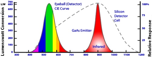
The first commercially usable LEDs were developed in the 1960’s by combining three primary elements: gallium, arsenic and phosphorus (GaAsP) to obtain a 655nm red light source. Although the luminous intensity was very low with brightness levels of approximately 1-10mcd @ 20mA, they still found use in a variety of applications, primarily as indicators. Following GaAsP, GaP, or gallium phosphide, red LEDs were developed. These devices were found to exhibit very high quantum efficiencies, however, they played only a minor role in the growth of new applications for LEDs. This was due to two reasons: First, the 700nm wavelength emission is in a spectral region where the sensitivity level of the human eye is very low (Figure 2) and therefore, it does not “appear” to be very bright even though the efficiency is high (the human eye is most responsive to yellow-green light). Second, this high efficiency is only achieved at low currents. As the current increases, the efficiency decreases. This proves to be a disadvantage to users such as outdoor message sign manufacturers who typically multiplex their LEDs at high currents to achieve brightness levels similar to that of DC continuous operation. As a result, GaP red LEDs are currently used in only a limited number of applications.
As LED technology progressed through the 1970’s, additional colors and wavelengths became available. The most common materials were GaP green and red, GaAsP orange or high efficiency red and GaAsP yellow, all of which are still used today (Table3). The trend towards more practical applications was also beginning to develop. LEDs were found in such products as calculators, digital watches and test equipment. Although the reliability of LEDs has always been superior to that of incandescent, neon etc., the failure rate of early devices was much higher than current technology now achieves. This was due in part to the actual component assembly that was primarily manual in nature. Individual operators performed such tasks as dispensing epoxy, placing the die into position, and mixing epoxy all by hand. This resulted in defects such as “epoxy slop” which caused VF (forward voltage) and VR (reverse voltage) leakage or even shorting of the PN junction. In addition, the growth methods and materials used were not as refined as they are today.
High numbers of defects in the crystal, substrate and epitaxial layers resulted in reduced efficiency and shorter device lifetimes.
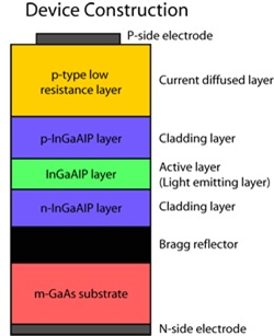 InGaAlP LEDs took a further leap in brightness with a new development by Toshiba, a leading manufacturer of LEDs. Toshiba, using the MOCVD (Metal Oxide Chemical Vapor Deposition) growth process, was able to produce a device structure that reflected 90% or more of the generated light traveling from the active layer to the substrate back as useful light output (Figure 4). This allowed for an almost two-fold increase in the LED luminance over conventional devices. LED performance was further improved by introducing a current blocking layer into the LED structure (Figure 5). This blocking layer essentially channels the current through the device to achieve better device efficiency.
As a result of these developments, much of the growth for LEDs in the 1990’s will be concentrated in three main areas: The first is in traffic control devices such as stop lights, pedestrian signals, barricade lights and road hazard signs. The second is in variable message signs such as the one located in Times Square New York which displays commodities, news and other information. The third concentration would be in automotive applications. The visible LED has come a long way since its introduction almost 40 years ago and has yet to show any signs of slowing down. A Blue LED, which became available in production quantities in the 1990’s, resulted in an entire generation of new applications. Blue LEDs because of their high photon energies (>2.5eV) and relatively low eye sensitivity have always been difficult to manufacture. In addition the technology necessary to fabricate these LEDs is very different and far less advanced than standard LED materials. The blue LEDs available today consist of GaN (gallium nitride) and SiC (silicon carbide) construction with brightness levels in excess of 10,000mcd @ 20mA for GaN devices. Since blue is one of the primary colors, (the other two being red and green), full color solid state LED signs, TV’s etc. have become commercially available. Other applications for blue LEDs include medical diagnostic equipment and photolithography.
InGaAlP LEDs took a further leap in brightness with a new development by Toshiba, a leading manufacturer of LEDs. Toshiba, using the MOCVD (Metal Oxide Chemical Vapor Deposition) growth process, was able to produce a device structure that reflected 90% or more of the generated light traveling from the active layer to the substrate back as useful light output (Figure 4). This allowed for an almost two-fold increase in the LED luminance over conventional devices. LED performance was further improved by introducing a current blocking layer into the LED structure (Figure 5). This blocking layer essentially channels the current through the device to achieve better device efficiency.
As a result of these developments, much of the growth for LEDs in the 1990’s will be concentrated in three main areas: The first is in traffic control devices such as stop lights, pedestrian signals, barricade lights and road hazard signs. The second is in variable message signs such as the one located in Times Square New York which displays commodities, news and other information. The third concentration would be in automotive applications. The visible LED has come a long way since its introduction almost 40 years ago and has yet to show any signs of slowing down. A Blue LED, which became available in production quantities in the 1990’s, resulted in an entire generation of new applications. Blue LEDs because of their high photon energies (>2.5eV) and relatively low eye sensitivity have always been difficult to manufacture. In addition the technology necessary to fabricate these LEDs is very different and far less advanced than standard LED materials. The blue LEDs available today consist of GaN (gallium nitride) and SiC (silicon carbide) construction with brightness levels in excess of 10,000mcd @ 20mA for GaN devices. Since blue is one of the primary colors, (the other two being red and green), full color solid state LED signs, TV’s etc. have become commercially available. Other applications for blue LEDs include medical diagnostic equipment and photolithography.
