
Custom LED Emitters
Utilizing our 35 years of experience in optoelectronics, Marktech’s customization process focuses on customer needs and applications. Instead of using standardized–but perhaps non-optimized–parts, Marktech allows advantageous custom product variations to enhance your product design.
Custom packaging and electrical sorting of product offer further differentiation. Marktech provides the designer with insights concerning custom variations–variations that optimize electrical, optical, and thermal characteristics–without the need for large volume commitments. In addition to our headquarters in New York where we have both our design engineering staff and complete testing department for all optical and electrical parameters we also have two manufacturing facilities in California and Japan. Marktech is a vertically-integrated company, allowing us to produce emitter components quickly, this decreasing your time to market. We can even produce your entire package in the United States.
To solve your needs, Marktech engineers will discuss with you:
- Application needs specific to your project
- Optimization of component and assembly packaging, technology, thermal and electrical parameters
- Manufacturing of dedicated end-products in support of your specifications and needs
Available products have wavelengths varying from 280nm (UV) through visible (440 to 700nm) to short wavelength infrared (up to 3000nm). Our online Product Selector Guide helps in the selection of emitter wavelengths, while also indicating compatible detectors. Tight binning by Marktech can provide uniform color characteristics to optimize the application and mating detectors’ sensitivities, providing process-controlled, uniform product solutions.
LED drive current and temperature
Optimal drive current and temperature minimize degradation/ lifetime effects.
Forward current vs. ambient temperature:
Figures 1 and 2 show an example in which the current is derated to take temperature into account. CREE technical data for LED lamps usually shows the permissible current values against temperature. Refer to this information when planning a new design.
The following example describes how to derate for temperature when designing:
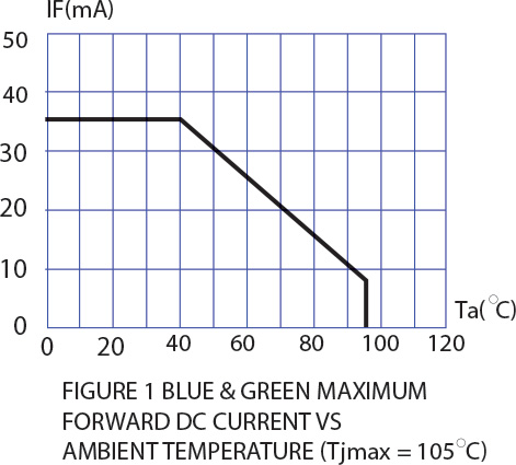
Figure 1 – Specified by design (25 mA) exceeds permissible value at 70C high temperatures
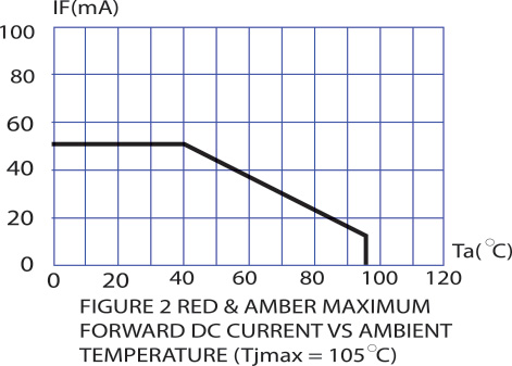
Figure 2 – Specified by design (25 mA) is within permissible value at 70C high temperatures
LED lamp example
- An LED lamp is to be used at an ambient temperature of 25°C.
- To obtain the required luminosity, set the LED lamp current to 20 mA.
- The guaranteed operating temperature range for the equipment is -10° to +70°C.
- If the current is derated for temperature, as shown in Figure 1, at 70°C the LED lamp current must be set to 20 mA or less. Hence a design that yields an LED lamp current of 25 mA is not permitted. However, some other types of LEDs that emit the same color have their current derated to take temperature into account, as shown in Figure 2. Since those LEDs can maintain a current of about 30 mA at a temperature of 70°C, they satisfy the above design conditions.
Derating for longevity
Characteristically, the luminous intensity of LEDs gradually decreases over the life of the LED. The rate at which the luminous intensity falls varies according to the material used and the forward current at which the LED is driven. The larger the current, the greater the diminution of luminosity. Thus, when setting the forward current of the LED lamp, do not determine the setting solely from the temperature characteristics, as in the above example, but consider also longevity characteristics. An effective way of improving the longevity characteristics is to set the forward current of the LED lamp relatively low.
Chip mounting
Die attach and wire bonding
What chip mounting options are best-suited for your application? Simpler wire-bond techniques and conductive paste die attach are acceptable for low-power devices, but as power increases, increased thermal conductivity is needed to assist in lowering chip temperatures.
Die attach
- Conductive epoxy die attach: good for low/ medium power applications
- Soft solder die attach: good/ very good for low or high power applications
- Eutectic solder die attach: good/ very good for high power applications
- Advanced Eutectic (thermal compression bond Gold Silicon): very good for high power applications. Difficult to apply
Wire bonding
(Source: Hybond, a wirebonder manufacturer):
There are three types of wire bonding:
- Thermocompression bonding
- Thermosonic bonding
- Ultrasonic bonding
Thermocompression bonding: A process that involves the use of force, time, and heat to join the two materials by inter-diffusion. The wire (heated in some cases) is pressed against the hot surface (at 150° C or more) at high force for a limited period of time to achieve the bond. No friction is used. This process uses gold wire and a gold bond surface, and it was originally associated with ball bonding. To this day, there are still some people who will use the phrase “thermocompression bonding” as a synonym for ball bonding, even if it now uses ultrasonic friction.
Thermosonic bonding
A process that involves the use of force, time, ultrasonics, and heat to join two materials. The wire (heated in some cases) is pressed against the hot surface (at 150° C or less) at low force and vibrated for a limited period of time to achieve the bond. This process uses gold wire and a gold bond surface, and it was also originally associated with ball bonding because the first time ultrasonics were used as a bonding parameter, it was done with ball bonding.
Gold ball bonding
So-named because it is the bonding of a gold wire, which, in its initial stage, has a ball or sphere formed on the end. A “flame-off” is used to make the ball. Originally the flame-off was done with an open hydrogen flame which would rotate towards the end of the wire and melt it, creating a sphere at the end of the wire. Currently the ball is made with an EFO (electronic flame-off), which creates a spark to melt the end of the wire. This bonding process uses force, time, ultrasonics, and heat to make bonds. As of recent years, copper wire has begun to be used for this process, but equipment must have modifications to prevent oxidation of the wire and especially the ball during its formation at flame-off.
Wedge bonding: This process was originally exclusive to aluminum wire, and no heat was used to create bonds. With time, heat was added to the bonding surface and gold wire was used for thermosonic wedge bonding of the gold wire. This is now a common form of bonding gold wire or ribbon. It should be noted, however, that some people still use the phrase “wedge bonding” as a term for ultrasonic (explained below) and not thermosonic wire bonding. Regardless of the traditional meaning of the phrase “wedge bonding,” the thermosonic wedge bonding process uses force, time, ultrasonics, and heat to make bonds.
Ultrasonic bonding
A process that involves the use of force, time, and ultrasonics to join two materials. The wire is pressed against the surface (both at ambient temperature) at low force and vibrated for a limited period of time to achieve the bond. This process can be done with gold, aluminum, copper, palladium, silver, or platinum wire or ribbons and to bond surfaces of the same materials. Originally, this form of wire bonding was done only with aluminum wire, so to this day, there are still some people who will use the phrase “ultrasonic bonding” as a synonym only for aluminum wire wedge bonding, even if it now is used for gold wire wedge bonding and other materials as well.
Wedge bonding
This process uses force, time, and ultrasonics with the bonding surface at room/ambient temperature to make bonds. Although originally exclusive to aluminum bonding applications, today there are many other materials and alloys that can be bonded by the ultrasonic method, including some thought at one time to only be effective if heat was applied.
Peg bonding
This process uses force, time, and ultrasonics with the bonding surface at room/ambient temperature to make bonds. Although peg bonding is exactly the same as wedge bonding, and can be done thermosonically as well as ultrasonically, the main difference with the techniques described earlier is that in a peg bonder, wire is not fed from a spool of wire by the wire bonder. Instead, the wire or ribbon (or any conductor in general) is either pre-aligned over the bond pad or it is manually introduced under the bonding tool (peg) to be bonded. A more common name to this process is TAB (tape automated bonding) or single point TAB. Hybond has given the name “peg” to this type of bonding because naming it TAB would lead to the assumption that a tape-feeding mechanism would be included as part of the equipment, and in reality, it is not. The name peg is also given by Hybond because the tool used for bonding usually looks like a peg, just as the tool used in wedge bonding looks like a wedge.
Today, ultrasonic bonding is a different process from what it was originally thought to be. The concept of interfacial rubbing is not valid. Ultrasonic energy, when applied to metal to be bonded, renders it temporarily soft and plastic. This causes the metal to flow under pressure. The acoustic energy frees molecules and dislocates them from their pinned positions, which allows the metal to flow under the low-compressive forces of the bond. Thus heat at the bond site becomes a byproduct of the bonding process, and the external heat becomes unnecessary to form the bond. This is also called a “cold weld.”
The friction of the wire breaks up and sweeps aside some contaminants in the weld area exposing clean metallic surfaces that promote the metallurgical bonds. It is important, however, to begin with a clean surface to avoid difficulties or failures in bonding. In some cases, the ultrasonic scrubbing may not be able to remove contaminants, as in the case of lubricants.
It also was found that the bonding tool moves cyclically across the top of the wire. A regular flat tool may not grip the wire well enough, and this causes the wire to slip back and forth across the bond surface of the tool. For this reason, there are tools that are made with more porous materials, such as ceramic-metal alloys, or that have special features like cross-grooves or grids that assist in the gripping of the wire during ultrasonic and thermosonic bonding.
Lensing
Illumination patterns and output
Spatial radiation characteristics: Lenses determine the angle-dependent output power obtainable. Lens characteristics determine intensity peaks and coverage areas. Marktech products provide great choice in beam angle, and these need to be matched to the application and sensor needs. Marktech uses goniometer equipment to analyze these radiation patterns.
Luminous intensity and directional characteristics Relationship between luminous intensity units and directional characteristics. Luminous intensity is measured in candela (cd), and the radiance is measured in watts/steradian (W/sr). One steradian is the solid angle at the center of a one-meter-radius sphere subtended by a square meter of surface area. The steradian is a metric unit. The radiance of light is the amount of luminous flux propagated in a given solid angle, or the amount of incident. Hence, as the figures below show, the narrower the directionality of an LED lamp, the higher the luminous intensity of that lamp.
Hence, for an LED lamp of given directionality, the higher the emission efficiency of the chip, the higher the luminous intensity.
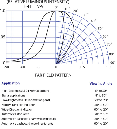
Application Viewing angle
High-Brightness LED information panel 15° to 30°
Signal applications 8° to 30°
Low-Brightness LED information panel 30° to 120°
Narrow-Direction indicator 30° to 60°
Wide-Direction indicator 60° to 120°
Automotive stop lamp 20° to 50°
Automotive dashboard narrow directionality 20° to 60°
Automotive dashboard wide directionality 60° to 120°
Visit Digikey for a listing of select Marktech emitter chips ranging from deep UV to the visible range to near-infrared and short wave infrared (SWIR).
View a full listing of Marktech emitter chips ranging from deep UV to the visible range to near-infrared and short wave infrared (SWIR).
Examples of customized products
Custom light rings
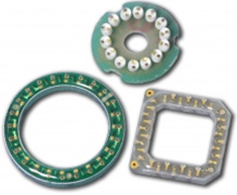
Custom light rings applications:
- Analytical instruments for the biochemical industry, medical and scientific analysis, endoscopy
- Critical illumination
- Security cameras
Marktech solution
Constructed with FR-4, metal core, or ceramic material, Marktech’s ring/chip offerings range from 280nm in the UV range though visible to near IR; white light ring options can be made with color temperatures ranging from warm (2600K) to cool (10000K). Emitter or detector chips–or a combination of both–can be included in custom light ring packages. In most cases, Marktech can test to plus or minus 1 nanometer. Their size offerings range from 4mm in diameter up to any required size.
Smaller size light rings are typically manufactured with COB [chip on board] technology, however, standard surface mount components such as 0805, 1206, and PLCC-type packages are also available depending on the optical performance required.
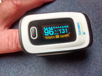
Pulse oximeter: Oxygen and pulse rate monitoring
Typical medical physicals now include quick and reliable readings of patient oxygen levels, findings that can be duplicated with home monitoring due to the low cost of access to the equipment. The oxygen levels of your blood are easily determined by a simple pulse oximeter where two different LED emitter wavelengths are used. Oxygenated blood tends to absorb light at 660nm; deoxygenated blood absorbs light better at 905nm. By making measurements and interpreting the results using Beer-Lambert’s law, the saturated peripheral oxygen level from your fingertip is quickly determined.
What’s needed
- Customized packaging of emitter parts to conveniently fit in a small package
- Optimization of the part wavelengths to increase accuracy
Marktech solution
Design, purchase, and modify LED-sorting equipment to bin LED products into tighter than +/- 1nm selected chips.
UV curing and drying of inks, adhesives, and coatings
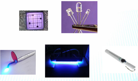
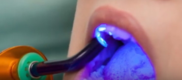
Ultraviolet LED emitter light curing is now used for applications ranging from dentistry to guitar finishes, including automotive, telecommunications, electronics, graphic arts, glass, and plastic decorating. Inks, coatings, and adhesives cured with UV LED light have dramatically improved physical properties. Traditional curing used highly inefficient and environmentally objectionable mercury lamps that could potentially damage the subject matter if misapplied. UV LEDs, on the other hand, are highly efficient and offer a longer-life alternative to standard bulbs. Heat output is easily controlled with LEDs while also lowering the time needed to cure, reducing the potential for damage to the cured object.
Advantages are
- Fast production speeds/increased capacity
- Dramatically reduced set-up/clean-up labor
- Environmental considerations for emissions and energy use
- Less floor space needed
- Increased manufacturing efficiency
Marktech solution
Marktech can optimize the emission wavelength for camphorquinone (CPQ) and other alternate materials that can be used as the curing photoinitiator. Packaging can be optimized for access to, for instance, small dental probes optimized for patient use.
For more information, see: http://blog.marktechopto.com/4-ways-uv-leds-are-changing-our-world/
Customized displays
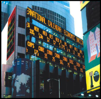
Times Square in New York City is an exciting, visually awesome area. Marktech has contributed to this area and to other large display applications with customized display capability including:
- Display visibility 12-16 blocks away and 60 feet below
- High quality – Zero defects /zero failures since 1996!
- Design solution of two-chip assembly with elliptical lens
- Cooperative manufacturing agreement with Toshiba
Bar code scanning
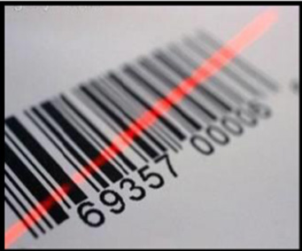
Bar code readers use emitters with:
- Consistent power output
- Repeatable wavelengths
Marktech solution
Design, purchase, and modify equipment to sort LEDs for power output, with selected/consistent binning.
SWIR (short wavelength infrared) emitter applications
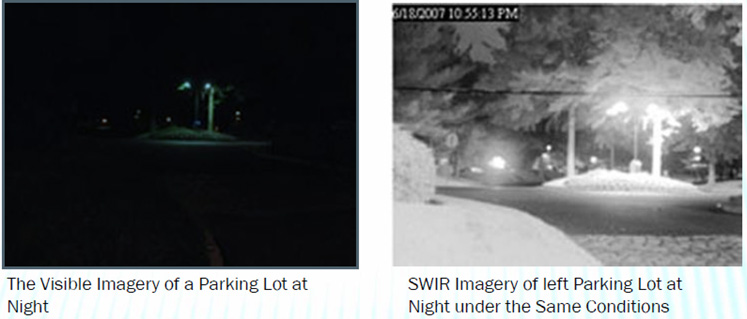
Short wavelength infrared (SWIR) LEDs are the latest addition to Marktech’s broad line of emitters. Marktech Optoelectronics is one of only a handful of manufacturers that supply emitters in the extended wavelength or SWIR range. Available in a variety of through-hole and surface mount packages, SWIR emitters satisfy a growing need for high-speed light emission in ranges not easily seen by standard detectors and are also being used for material and chemical analysis.
Typical industries served
Medical, security, military, communications, industrial, and agriculture
Common applications
The rapidly growing market for SWIR includes applications like produce inspection, security, surveillance, anti-counterfeiting, biomedical bioflorescence and blood chemistry analysis, night vision, safety equipment, currency validation, fiber optics, and inspection system devices.
SWIR detectors can help realize non-invasive imaging methods, for example, optical coherence tomography (OCT) systems, utilizing SWIR to exploit the low scattering properties of >1μm light to see the previously unreachable, thick parts of the cornea.
Marktech solution
Marktech’s standard product offerings includes both through-hole and surface mount packages with wavelengths from 1050nm to 1720nm and operating currents ranging from 20mA to 350mA for high-power applications. Higher wavelength ranges up to 3000nm are available in specific package types.
The Marktech extended wavelength standard SWIR package offerings include TO-46 flat, TO-46 lens, TOPLED PLCC4, SMD 1206, SMD 1206 Lens, and SMD high-power black. Custom package options are also available.
View Products
Find something you were looking for? Get a free no-obligation quote today.
Related Resources
Have a question? Contact Us
The possibilities are limitless. If you have a project requiring custom InGaAs or silicon photodiode detectors, custom LEDs, multi-chip packages of multi-wavelength LED emitters combined with optical detectors, or custom assemblies, then please contact us for help with selecting the correct devices for your design requirements. We work on projects of any size and quantity, and while we have hundreds of standard products – customizations are our specialty.
