
Photo Sensor Application Notes

Figure 2-2.1 – Principle of operation of optical sensor
Design Procedures For Optical Sensor Circuits First, obtain values of RE and RL. In Figure 2-2.1(a), when the forward voltage drop of an LED is VF, current IF flowing to the LED is given by: (1) IF = (VCC-VF) / RE and it is necessary to satisfy (2) IF = IF (MAX) (Ta = TOPR (MAX)) From (1) and (2), RE is given by the following formula: (3) IF = (VCC-VF) / IF (MAX) As can be seen in Figure 2-2.2, the larger IF is, the more optical output IE will be produced and therefore, it is necessary to calculate IF (MIN) by taking the fluctuation of allowable loss of IF and IE into consideration after deciding RE. Proper Value of RL: Obtain the upper limit value of RL In Figure 2-2.1(b), when a light cutoff plate is inside, photo electric current IL produced by light emission from the LED does not flow to a photo transistor but leakage photo current IL’ and dark current, Id, only flows. Potential of the collector VOH at this time is: VOH = VCC – RL x (Id +IL’) However, it is assumed that input/output current to/from the next stage can be disregarded.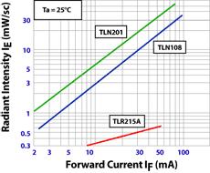
Figure 2-2.2
Since Id increase rapidly with ambient temperature rise as shown in Figure 2-1.5, assuming the high level input voltage of the next stage is VIH, it is necessary to satisfy the following: VIH < VOH at Ta = Topr (MAX) RL = (VCC – VIH) / (Id + IL Then, obtain the lower limit value of RL. When the light cutoff plate is not inside, light is received by the photo transistor and light current IL and the above mentioned Id + IL’ flow to the photo transistor. Normally, unless: IL = Id + IL’ it becomes difficult to discriminate existence of a light cutoff plate from the viewpoint of S/N ratio, the collector potential VOL at this time is (4) VOL = VCC – RL (IL + Id + IL’) Assuming that the low level input voltage to the next stage is VIL’ it is necessary to satisfy (5) VIL > VOL Formulas (4) and (5) must be satisfied even at the lower limit value of IL. The lower limit value IL (MIN) is: IL (MIN) = CTR (MIN) x Dt x DTa x Dn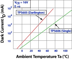
Figure 2-1.5
Dt: CTR degradation factor during operation (Fig. 2-1.7) DTa: CTR temperature variation (Fig. 2-1.6) Dn: CTR variation from dust and dirt From formulas (4) and (5), RL = (VCC – VIL) / (IL(MIN) + Id + IL’) The smaller RL is, the shorter the switching time will become. HOW TO OBTAIN COUPLING CHARACTERISTICS OF LIGHT EMITTING AND RECEIVING DEVICES In the following, coupling characteristics of light emitting and detecting devices are calculated as the initial design to see if they are applicable. Then, as the second step a method to check actual operation, etc. is presented. Initial Design Coupling characteristics of representative product is shown in Figures 2-4.1 ~ 2-4.3. Such characteristic diagrams as these are somewhat different depending upon the combination of light emitting and detecting devices. Generally, when d > 1 cm or more in the following calculating method, these characteristics can be obtained roughly without investigating them individually.
(left)Figure 2-4.1 – Coupling characteristics of TLN108 and TPS601A (right)Figure 2-4.2 – Coupling characteristics of TLN105B and TPS703

Figure 2-4.3 – Coupling characteristics of TLN107A and TPS608A
First, read radiant intensity IE (MIN) of a light emitting device and light current IL (MIN) of a light detecting device according to conditions shown in the data sheet. As radiant intensity IE (mW/sr) is equivalent to radiant incidence EO (mW/cm2) radiated on an area 1 cm2 at distance 1 cm, obtainable radiant incident E (actual) at a distance d cm is obtained by the following formula: E (Actual) ~ IE/d2 (mW/cm2) Assuming that the radiant incidence of a light detecting device at the light detecting sensitivity conditions is E light current IL (actual) in the coupled state is obtained as follows: IL (actual) = IL x(E (actual) / E) When the received light current is very small and it is difficult to design the latter stage circuit, increase the DC forward current IF of the light emitting device or increase radiant intensity IE (mW/sr) by pulse forward current. As an example make an examination under the following conditions: Emitter: IE(MIN) = 1 mW/sr at IF = 20 mA Detector: IL(MIN) = 20 μA at E = 0.1 mW/cm2, VCE = 3V Distance between Emitter and Detector: d = 1.5 cm E (actual) (MIN) = IE / d2 = 1 x (1/1.52) = 0.44 mW/cm2 (MIN) IL (actual) (MIN) ~ (E (actual) / E) x IL (MIN) = (0.44 / 0.1) x 20 μA = 88 μA As IL (actual)(MIN) is 88 μA, it is not possible to drive TTL directly, but a C-MOS IC can be connected. Then, while the load on a light receiving device is decided according to supply voltage, its switching speed depends strongly upon the load value and it is necessary to check it in advance. Application Circuits of Photo Sensors Application Circuits of Infrared LEDs Since power output Po, of an infrared device depends on the LED forward current, IF, the On-Off status of the output can be addressed through control of forward current. Representative lighting methods such as DC lighting, etc. and precautions for design are explained here. Shown in Fig. 3-1.1 is the basic circuit for lighting when DC power is used. IF in this case is expressed by the following formula: IF = (VCC – VF) / R VCC : Supply voltage VF : Forward voltage of LED IF : Forward current flowing to LED PHO Lighting Circuit DC(Left To Right) Figure 3-1.1 – DC Drive unit Figure 3-1.2 – Constant current drive circuit Figure 3-1.3 – Multi LED drive circuit
Shown in Fig. 3-1.2 is a circuit covering the variations of VF of an LED with Transistor. IF in this circuit is expressed by the following formula: IF = (VB – VBE) / R3 VB : Base voltage VBE : Base to emitter voltage R3 : Emitter resistance Further, it is possible to reduce the temperature dependency of the output by properly setting VBE and VB in this circuit. When output power is insufficient or the light receiving device is located too far away, it is possible to complete the circuit through a series or parallel connection as shown in Fig. 3-1.3. In this case, IF = (VCC – nVF) / R (series connection) IF = (VCC – VF) / R (parallel connection) AC Driving Shown in Fig. 3-1.4 are the basic circuits for nearly half-wave AC lighting. Generally, there are two driving methods. Both of them use a protective diode to protect the LED from reverse voltage. In (a), this protective diode is reverse voltage type corresponding to supply voltage VCC, and in (b), reverse voltage of the protective diode should be about twice the forward voltage of an infrared LED.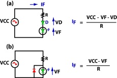
Figure 3-1.4 – AC drive circuit
Pulse Driving Many advantages are obtainable when the optical signal is changed to pulse modulated light. The following are considered: When the duty ratio of a pulse modulated signal is small, the instantaneous light output of a light emitting device increases, the optical signal is discriminated from ambient light and S/N ratio improvement is ensured. When a battery is used as a power source, the power consumption of a device can be reduced and therefore, battery service life is extended. RC coupling with the next stage in the light receiving section becomes possible and the effects of dark current increases resulting from a temperature rise can be avoided. This pulse driving system is designed in combination with TTL or C-MOS and Tr, etc. In the circuit shown in Fig. 3-1.5, it is necessary to pay attention to the electrical characteristics of IOL of a TTL or C-MOS device since excessively large currents cannot be applied to satisfy IF < IOL. To apply a higher current, it is necessary to use a buffer IC with a high output current capacity as shown in Fig. 3-1.6 or to install a transistor externally. IOL and VOL characteristic of TTL, C-MOS and buffer IC are shown for reference.
Figure 3-1.5
Application Circuits of Photo Transistors Basic Circuit A basic circuit for a photo transistor is shown in Fig. 3-2.1 Load resistance RL is selected by taking the dark current temperature characteristic of the photo transistor into consideration. If RL is too large, a photo transistor may be turned ON only by dark current at high temperature. For instance, when Photo Transistor TPS601A is operated at Ta = 100°C, dark current may become about 100 μA. When RL is set at 50 kW at VCC = 5V, TPS601A is completely turned to the ON state by the increase in dark current.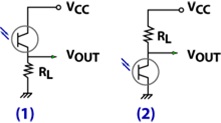
Figure 3-2.1 – Basic circuit of photo transistor
Bias Circuit of Photo Transistor with Base Terminal The effects of a base to emitter resistor RBE on dark current as well as light current are shown in Fig. 3-2.2 (a) and (b). Normally, the dark current of a photo transistor is as small as several nA at normal temperature and it is possible to reduce dark current further by inserting a resistor RBE between the base and emitter to bypass leakage current through the collector to base junction point. If RBE is made excessively small, the apparent hFE of a photo transistor is reduced and the required light current IL cannot be obtained, therefore, an RBE of more than 1 MW is appropriate.
Figure 3-2.2 (a) – Decrease of dark current by RBE / Figure 3-2.2 (b) – Change of light current by RBE
Further, it is possible to set the operating point of a photo transistor at a proper level by using the base terminal. Linearity of illumination-light current characteristics in this case has been improved considerably when compared with the case where base bias current is zero. In addition, there is a bleeder type bias method shown in figure 3-2.4, which improves thermal stability at the DC operating point experimentally, 2 ~ 10 MW is considered proper for a value of RB. This is to apply almost all light current IL of a photodiode at the collector and base junction points to the base of a photo transistor by raising impedance at the base.Figure 3-2.4 (b) – Bleeder type bias method
Temperature Compensating Circuit The light current IL and dark current Id of a photo transistor have a positive temperature coefficient. In particular, dark current increases exponentially as shown in the individual technical data sheets. Therefore, to obtain stable operation at ambient temperatures of 50 ~ 60°C , temperature compensation for dark current and photo electric current of a photo transistor becomes necessary. The circuit shown in Figure 3-2.5, uses a negative temperature coefficient retained by the forward voltage VF of a diode. When a photo transistor having no base terminal is used, a method to compensate for output voltage would be to reduce the load resistance of the photo transistor by using a thermistor as shown in Fig. 3-2.6.
Figure 3-2.5 – Temperature compensation circuit using resistance diode
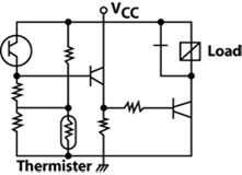
Figure 3-2.6 – Temperature compensation circuit using thermister
Basic Amplifier Circuit Shown in Fig. 3-2.7 (a) is a Darlington connection using a NPN transistor and Fig. 3-2.7 (b) is a Darlington connection using a PNP transistor. In both circuits, light current is increased by hFE times and output current IC becomes hFE . IL
Figure 3-2.7 – Amplifier circuit for photo transistor
Fig. 3-2.8 shows examples of basic circuits using amplification by an operational amplifier.

Figure 3-2.8 – Amplifier circuit with operational thermister
Improvement of Switching Speed When voltage amplification is raised by increasing load impedance as light current of a photo transistor is small, switching speed characteristic may be sacrificed as a reverse effect. As a remedy, there are methods to obtain switching speed characteristics which are relatively independent of the size of the load by converting impedance through PNP transistor based circuits (Fig. 3-2.9 (a)) or cascade connection of NPN transistor (Fig 3-2.9 (b)). Test methods are applicable to a high speed pulse modulated light detection circuit for a photo electric switch/high speed tape reader.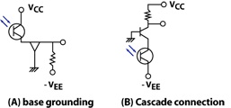
Figure 3-2.9 – Examples of frequency characteristic improvement
Analog Usage Photo transistors provide higher sensitivity than photo diodes as they are equipped with an amplification function internally; however, the sensitivity fluctuates significantly depending upon the difference in amplification factors. Therefore, it is necessary to either use a variable resistor to correct the sensitivity or purchase a product which is pre-selected for a specific sensitivity rating.
Figure 3-2.14
Shown in Fig. 3-2.14 (a) is a circuit controlling the current of a transistor amplifier. The collector current of a photo transistor controls the base of the next stage transistor of which emitter is grounded. Fluctuation in the photo transistor’s sensitivity is controlled by feedback resistor RE in the emitter circuit. Shown in Fig 3-2.14 (b) is a circuit controlling the voltage of a transistor amplifier. The collector current of a photo transistor generates a voltage for controlling a latter stage transistor by a variable resistor. A transistor is an follower and fluctuations between individual photo transistors are corrected by a variable resistor RA. Therefore, photo transistor’s switching time is changed by RA. Application Circuits of Photo Diodes In combination with infrared LEDs, photo diodes are used in two ways; digitally to detect the existence of light and analog to detect the quantity of light. Digital Usage As response speed is fast, photo diodes are suitable for high speed switching. On the other hand, however, since light current is small, it is necessary to use a FET with high input impedance as shown in Fig. 3-3.1 (a) or a circuit with high amplification as shown in Fig. 3-3.1 (b). To raise amplification, an operational amplifier is used. When high speed response is required, it is necessary to select an amplifier for appropriate high speed applications.
Figure 3-3.1 – Amplifier circuit of phoro diode (digital usage)
Analog Usage Illuminance and photo electric current characteristics of photo diodes are more close to linear than those of photo transistors and photo diodes can be said to be a product that is easily used in analog applications. For this type of usage, there is linear amplification and logarithmic amplification.
Figure 3-3.2 – Amplifier circuits of photo diode (analog usage)
Application Circuits Of Reflective Type Photo Sensors The reflective type photo sensor is available in two types; focus type and non-focus type. The proper type should be selected based upon the application. As can be seen from the respective basic detecting position characteristics shown in Figs. 3-5.1 and 3-5.2, the black and white boundary surface position detecting characteristic of the focus type is sharper than that of the no-focus type. Therefore, the focus type is superior to the non-focus type for bar code detection applications. However, the small non-focus type is effective for the detection of objects.
Figure 3-5.1 – Example of non-focus type detection position characteristic

Figure 3-5 – Reflection type photo sensor basic detection circuit
Since it is necessary for the reflection type of photo sensor to digitally output the existence of a detected object, a comparator circuit is connected at the next output stage of the reflection type photo sensor as shown in Fig 3.5-4.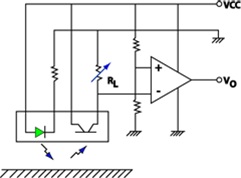
Figure 3-5.4 Connection circuit of reflection type photo sensor with comparator
Application design of the reflection type photo sensor is more difficult than the transmission type photo sensor because:- Reflection factors of reflecting substances are different from each other
- Distances of reflecting substances are easily controllable
- Both light emitting and detecting surfaces are on the same plane and susceptible to the effects of external light, and leakage current increases.
- Therefore, it may be said it is better to design a transmission type photo sensor if possible.
View Products
Find something you were looking for? Get a free no-obligation quote today.
